Theory of transistor MOS
1) Typology of transistor MOS:
There are the transistors nMOS and pMOS it is of the type enhancement (…for which it is necessary to apply a tension of opportune sign to the gate ones to the aim to form the channel) that depletion (…for which the channel is formed also for VGS = 0).
2) Principle of operation nMOS:
A substrate is had p-doped in which they are gains two equal traps to you n-doped, one for source and the other for the drain, they are separate you from a space over to which there is the oxide and the gate ones, for VDS = 0 the following situations are had:
to) Accumulation: applying a negative tension to the gate ones regarding the substrate, the present gaps in it will be recalled towards oxide therefore in pressed its will be had accumulate of gaps and therefore current in how much does not slide has two splices pn in contropunta.
b) Svuotamento : applying a positive but inferior tension to the tension of threshold VT is had that the gaps come removed give to oxide close therefore create one emptied region of bearers
c) Inversione : applying a advanced positive tension to Vthe T is had that they come recalls electrons to you from the substrate that therefore come to constitute a channel that puts in contact source and drain.
In case VDS ¹ 0 it is necessary to hold account is of VDS that of VGS in order in particular to establish the region of operation of the nMOS if VGS < VT is in interdiction in how much the channel is not formed from the side of the drain while for VGD< VT it is in saturation and the channel is not only formed in the pressed ones of the drain. In intermediate situations, the channel is formed and it is in region of triodo or not-saturation.
3) Tension of threshold VT :
The tension of threshold VT is due to the fact that is necessary a positive tension
leggermente in order to remove the majority bearers and to recall the
minority ones, it is worth ![]() where
where  is the tension of threshold for a not present MOS that
difference of function job between gate and substrate being
  upgrades them of the bulk and
 ![]() loads
with the bulk while
loads
with the bulk while  is the tension of flat band
with Qfc loads due to the
superficial states. Alla light delle previous chosen relations
is obvious that a time the materials for the gate ones and for the
substrate, Vt it can have varied
acting on NTo , Qfc (…by means of
impiantazione of Ionian) and Cox (…using different materials insulators for the
gate ones).
4) Model base of the nMOS:
to) interdiction : the DS = 0 for VGS < Vt
b) not saturazione:
 per 0
< VDS < VGS - Vt
c) saturazione :  per
0 < VGS - Vt < VDS
being  the gain factor.
5) regarding Effects of 2° the order the NMOS:
to) Body effect
The substrate of the nMOS normally is connected to
VSS , that determines Va SB = 0 however in some logical
structures as that one of the Nand can be necessary to place in
cascade of the nMOS and therefore for some of they necessarily
SB ¹0 will be had V. The effect of this tension is to increase
the threshold tension, in fact this VSB is behaved as an inverse polarization and therefore
neutralizes the free charges and increases to the extension della
region of depletion, of it derives that in order to form the gate
channel it is necessary to more apply al one elevated tension.
In particular the expression of the Vt that it holds account of Vthe
SB is ![]() comprised with g between 0.4 and 1.2 .
comprised with g between 0.4 and 1.2 .
b) Operation sottosoglia
For VGS < Vt it is in interdiction howeverthe DS also being much small it is not null and it has a exponential course that can be used for systems to low consumption.
c) Modulation of the length of the channel
In saturation the channel completely is not
formed but of it small extension from the side of the drain lacks one,
that determines a lessening of L and consequently an increase is of
relationship W/L that of b ,
therefore an expression ofthe DS that it holds account of this effect is  comprised with l between 0.02V-1 and 0.005V-1 .
d) Variation of mobility
Mobility diminishes with the drogaggio and with the increase of the temperature, moreover mobility of electrons is double regarding mobility of gaps.
and) Effect Tunnel
In the case that the oxide of gate is a lot until
you can be passage of current from the gate ones is towards the source
that towards drain for effect the Tunnel second the equation  .
.
f) Punchthrough
If the tension applied to the drain is much elevating, it can be had that the emptying region extends until to the source, and therefore can slide one independently current from the tension of gate.
g) warm Electrons
When the length del gate is much small and the transistor is in saturation has an elevated electric field dal side del drain, this gives to place to electrons many energetic sayings warm electrons which goes to impattare with present gaps nel drain and they push to them towards the substrate or in some cases towards the gate ones giving therefore place to delle currents.
6) Model of the nMOS for small marks them:
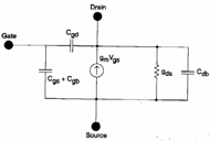 In this model the abilities between the various clips are
present all, an escape conductance is obtained supposing that the MOS
works in not-saturation region and therefore deriving regarding VDS
  the it
is obtained
 ![]()
While for transconduttanza gm it is necessary to derive IDS regarding VGS .
7) Diode valve:
It is a splice pn for which the expression of the current
is  therefore in the case of inverse polarization
has only the inverse running weak persons the due to the minority bearers while in the case of direct
polarization a exponential course of the current in function of
tension V has itself applied to i heads of the diode valve.
8) BJT:
It is a sandwich npn or pnp for which the following model is had:
to) Interdizione : both the splices are polarized inversely, of it it derives that it does not slide current between emettitore and collector.
b) Attiva : the splice base-emettitore is directly polarized therefore its heads is had approximately 0,7V while the splice base-collector is polarized inversely, in this casethe C = bthe B .
c) Saturazione : both the splices are polarized directly, it is had that to the heads of the splice base-emettitore there are approximately 0,7V while between collector and emettitore there are 0,2V.
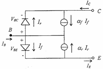 A model that very represents the operation of the BJT is
the model of following Ebers-Moll:
For which it is reached quickly the  expression where VTo it is the tension of Early due to the reduction of the
length of the base and is worth approximately 50V.
9) Inverter nMOS with saturated cargo nMOS to emptying:
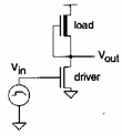 A nMOS is had having as loaded a nMOS depletion which it
comes made to constantly work in saturation simply cortocircuitando
the gate ones with the following escape according to outline:
for famous it that ![]() , in order to
determine the tension of income for which the commutation from high to
bottom is had, is necessary to suppose both the MOS in saturation and
uguagliare the currents,
, in order to
determine the tension of income for which the commutation from high to
bottom is had, is necessary to suppose both the MOS in saturation and
uguagliare the currents,  is obtained where
 ![]() . Evidently being for pull-down
. Evidently being for pull-down ![]() the for having the running principle it is necessary to
reduce Vtpd but it cannot be
reduced too much otherwise cannot be had Vout inferior to it and to extinguish the MOS, in kind
chooses Vtpd = 0.2VDD , analogous for the pull-up
the for having the running principle it is necessary to
reduce Vtpd but it cannot be
reduced too much otherwise cannot be had Vout inferior to it and to extinguish the MOS, in kind
chooses Vtpd = 0.2VDD , analogous for the pull-up ![]() is had therefore is necessary to increase Vtpu for having the running principle but
that implies to increase the
is had therefore is necessary to increase Vtpu for having the running principle but
that implies to increase the ![]() relationship with
consequent increase of the occupied area therefore imposing the
equality of the currents between pull-up and pull-down V tpuis obtained = 0.8VDD but in kind is reduced to us to 0.6VDD that it implies that if
INV is desiredV =
0.5VDD is necessary to
have
relationship with
consequent increase of the occupied area therefore imposing the
equality of the currents between pull-up and pull-down V tpuis obtained = 0.8VDD but in kind is reduced to us to 0.6VDD that it implies that if
INV is desiredV =
0.5VDD is necessary to
have![]() .
.
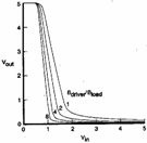
as one looks at the characteristic is that one of a inverter that it carries out the maximum excursion and that slope has one much elevating or in order better to say a gain elevated in correspondence of the high passage downstairs.

10) Inverter pseudo-nMOS:
Draft of a inverter in which the pull-up it is constituted from a pMOS that it is behaved like a nMOS
11) Inverter CMOS:
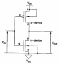
It is a inverter with optimal performances in how much guarantees the complete excursion of Vthe DD and one of the two MOS does not dissipate power in the stable states in how much is always interdetto therefore not is never one logon directed between VDD and VSS . The analysis is carried out subdividing the study in 5 regions of operation that determine considering that the MOS can be found in interdiction, linear region or saturation. We consider one Vin crescent from VSS to VDD :
0 < Vin < Vtn : the nMOS is interdetto therefore the current that crosses it is null as pure therefore the current must is null that crosses the pMOS which instead it is in active region therefore VDS = 0 and VOUT = VDD .
Vtn < Vin < VDD/2 : the nMOS enters in saturation while the pMOS it is in linear region, uguagliando the two expressions ofthe DS previa substitution of VGSp = Vin â?"VDD e VDSp = Vout â" VDD obtains the expression of Vout .
Vin = VDD/2 : both the MOS are in saturation, draft of one be unstable valid only for this value of the income tension, the value of the escape tension are not determined univocamente.
VDD/2 < Vin < VDD Vtp : the nMOS is in linear region while the pMOS it is in saturation, uguagliando the two currents obtains the expression of the Vout .
Vin > VDD - Vtp : the nMOS is in linear region while the pMOS it is interdetto, ci² determines that Vout = VSS
It is from observing that we have placed V
arbitrarilyinv = VDD/2 while its expression is gained
imposing the saturation for both the MOS, has  from which evince that to growing of the relationship of i b the Vinv it diminishes while the ripidità of the curve remains
unchanged, however is chosen advised to have the
b equal, in such a way in fact loads and the
discharge of the cargo ability is temporarily equivalents.
12) Margins of noise:
We consider inverter a CMOS that pilot a second inverter
CMOS, the escapes of the 1° advanced to VOL comes considers low levels you while those advanced
ones to VOH come considered
high levels. For the 2° inverter instead, the inferior incomes
to V they come considers low levels
you while those advanced ones to VIH come consider high levels you, naturally in order to avoid
of having a indeterminata zone convene that VIH = V , values that
can be determines you from the characteristic curve characterizing the
having points slope â?"1 (…than then corresponds to the
gain being the curve that expresses Vaccording to out Vin). They come defined the noise margins that say how
much to us can be elevated the noise in order not to recognize a level
like an other, have ![]() e
e ![]()
13) Inverter BiCMOS:
It is a inverter particularly adapted laddove must be piloted great cargos to high speed, such performances in fact can be only obtained with one exited BJT, the outline is following:
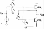
for Vin = 0 P 1is had on that therefore it after all sends in conductionNPN the 1 whileNPN 2 is interdetto fromN 3, escape door to VDD â " VBE . For Vin = 1 N 1is had on and therefore NPN1 is interdetto while N2 sends in 2 conductionNPN and therefore the escape door to the value VCEsat that is to approximately 0,2V, therefore the excursion of this inverter is not maximum and creates problems in the case of many inverter in cascade.
14) Transmission Gate:
 E' a device a lot used in order to realize multiplexer and
exited tristate, the study of its operation comes carried out
separately for the nMOS and for the pMOS supposing that there is an
ability connected to the escape, it is had:

If S=0 the nMOS is blocked independently from the value of the income while for S=1 if Vin= the 1 condenser it is loaded and being VGD = 0 it is in saturation, but DD loads does not arrive until toV DD in how much the nMOS passes in interdiction forV out =V- Vt Quando Vin pass to 0 the condenser must be unloaded, the source more negative of the nMOS is the clip and therefore that one of income therefore VGS initially is equal to VDD > Vt therefore the channel is formed from the side of the source and it it is also from the side of the drain in how much has VGD > Vt , it is therefore in region of triodo and the condenser discharge completely in how much from the expression ofthe DS is had that it only cancels itself if VDS = 0. From the previous ones it is deduced that the nMOS he is ideal in order to concur the passage of the low levels, but insufficient for the high levels.

If - S=1 the pMOS is blocked independently from the value of the income while for â?"S=0 if Vin= the 1 condenser are loaded, in this case VSG > VT and therefore the pMOS it is always in conduction and the condenser loads until to VDD . When Vin = 0 the condenser must be unloaded but when it reaches value Vt , interdice therefore it is achieved some that the pMOS it is behaved well in the transfer of the high levels and badly in the transfer of the low levels.
After all the transmission gate if S=0 has an escape in high stiffness that leaves the condenser its value of it loads while if S=1 the high levels come it passes to you in escape from the pMOS while the low levels come pass to you from the nMOS.
