Circuits CMOS and logical plan
1) Causes of malfunctioning of one door CMOS:
to) insufficient Feedings and/or noise on the same ones
b) Noise in income
c) out of order Transistors and/or interconnections
d) Divisions of load not previewed
and) Temporizzazioni wrong
2) critical Distances us and they optimization:
Draft of distances discs of a valve which can be is characterized to you for experience or by means of of the timing analyzers, once it characterizes to you, it can be acted on they to architetturale level, logical level acting on the type of gate and fan-in and fan-out, to level circuita them acting on the dimensions of the MOS or using various styles from the CMOS, and finally to level of layout.
3) Considerations on the optimization of the critical distances us to logical level:
Fan-in of a logical door that is the n° of incomes that it can have it is well is limited between 2 and the 5 moreover doors nand are from preferring themselves to the nor in how much characterized from a smaller delay, in the case in which it is equally decided to use them convene ridurne fan-out that is the number doors that can be piloted from the escape, in any case then inserting a inverter can be piloted a whichever number of doors.
Progettuali architectures
4) Full custom:
It consists in the planning and every optimization of single present MOS in the circuit, this of it reduces the complexity to a maximum of approximately 60 MOS. It is a slow process much and expensive one but it concurs to optimize area and performances.
The planning is articulated in following is made:
to) one schematic of the circuit is come true
b) the layout is planned
c) Fixed the designs rules taxes from the technology prechosen, uses a layout editor in order to realize the masks
d) a layout extractor leaving from the masks it supplies schematic a comprehensive one also of eventual dispositi to you you adorned to you, such schematic it comes simulated with SPICE and if the operation is corrected it passes to the production.
5) Cell Standard:
They come used of the cells present standards in the bookcase of the foundry, are cells to constant height and variable width in which is predefined the positions of incomes, escapes, VSS , VDD .
The planning is articulated in following is made:
to) choice of the bookcase and therefore of the foundry
b) the schematic one is come true using the members of the foundry who are seen like of the boxes black them.
c) By means of the Schematic- Capture comes more replaced the black-box with the cell adapted
d) digital Simulation them
and) From the schematic one the layout is obtained of the chip by means of a software of Placement Routing that carries out the optimization of the positions of the cells.
It is a faster planning in how much is worked to logical level but the costs are equally much high in how much are necessary from the 15 to the 20 masks.
6) Gate Array:
It is a planning based on the realization of easy riconfigurabili structures which include the greater part of are made realizzative, they are subdivided in particular in 2 classes:
MPGA : the foundry realizes a series of blocks base which must be interconnected between they by means of of the metalizations that come specified from the planner which leaving from the demanded function it realizes the opportune masks.
FPGA : the foundry produces a chip in which beyond to the riconfigurabili structures they are present of the programmabili interconnections, therefore it is not more necessary to realize of the masks. Such chip they are expensive but they can be reshapes to you by means of I affixed software to you.
7) Sea-of-gates:
In practical generalization of the layout is one of gate the Array, constituted from continuous lines of spreads n and p. Not there is space for the interconnections which come carried out through the MOS lines do not use you. Every logical door can be isolated from the adjacent door connecting the gate ones of the last MOS to VSS or to VDD.
8) logical Structures CMOS:
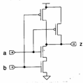
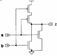
to) Logical complementary CMOS
 |
 |
 |
|
The main advantage is that the static dissipation is due exclusively to the currents of inverse saturation, moreover can operate to tensions many lowlands, between the main disadvantages instead there is that for whichever function they always come uses ugual a number you of pMOS and nMOS that sometimes is redundant. The main logical functions are:
Inverter Nand Nor
 b) Logical BiCMOS
It is a structure used for the stages of escape in how much being present of the BJT concurs to pilot cargos elevates to you and to increase the speed regarding the CMOS, an example of executed logical function with this structure is following:

c) Logical Pseudo nMOS and Multidrain
The pull-up it is constituted from a solo pMOS, that implies that the n° of MOS it uses you in order to realize a generic function is inferior to how many of would be necessary in order to realize it with the CMOS however that implies also that the static dissipation is higher in how much is of the logical conditions for which is a distance directed between VDD and VSS .
Logic CMOS Moltidrain is distinguished then in which the doors are connected in the configuration open-drain in analogous way to how much happen for the BJT in logic IIL.
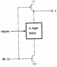 d) Logical dynamics CMOS
It is a logical structure nMOS whose exited precaricata to VDD from the one pMOS and conditionedly connected to VSS from one nMOS, in this way main advantage regarding the CMOS is that a clearly inferior number of doors is used Of it derives that the time of pull-up diminishes while it increases the time of pull-down. A defect is that the incomes can only vary during precarica it while they must be stable during the appraisal otherwise have effects of charge-sharing. Evidently an other dynamics door CMOS to single phase in how much cannot be connected in series when the clock the escape passes to the phase of appraisal that goes in income to the next structure can be found still high for via of the time of reduction that is small but not infinitesimal, after all has the loss of the data.

and) Logical clocked CMOS:
E' be developed essentially in order to realize CMOS to low dissipation but currently finds application mainly in those situations in which the problem of electrons is pressing âcaldiâ?.
In short they come inserted two MOS for the clock or to the center or in proximity of the feedings.

f) Logical I dominate
Draft of one logical dynamics on whose exited a CMOS is placed inverter which is concurred to place in cascade various doors also having clock to one a phase.

 One can be obtained logical statics by means of pMOS a
weak person (…to low gain) arranged as from figure which
it concurs the operations to vlf or statics in how much during the
phase of appraisal the escape even if is high with passing of the time
ends in order to unload itself, pMOS the weak person glielo prevents,
its impact is null in vhf in how much is not enough fast. Alternatively it can in such a way be connected the gate
ones of pMOS the weak person to the escape of the inverter creating a
latch
g) Logical I dominate NP
 The buffer present in I dominate can be eliminated
to pact to use of the dynamic structures with logic pMOS alternated to
dynamic structures with logic nMOS, because they come placed in
cascade is clear if it is believed that every structure of the sort
realizes a logical door and the escape of every door is in kind
connected to an other door.
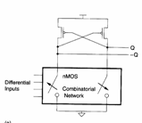
h) Logical Cascade Voltage Switch
2 switch are had nMOS complementary connected to a brace of pMOS intercross to you that they act as from pull-up. It is slower regarding the CMOS in how much the pMOS of the pull-up must fight against the nMOS of the pull-down. The advantage is that every logical function but to expenses of one can be realized greater occupied area and complexity. The performances can be improved by means of use it of a latching sense-amplifier.
Clocking Strategies
9) Consequences of the choice of the tipologia of clock:
The choice of the strategy of clock influences the n° of MOS to use for every element of memory and the n° of it marks them of clock distributing on the chip, therefore indirectly it determines the dimensions of chip and the dissipation.
10) characteristic Times of a registry:
TS = Time of Setup : indicates how much time before the forehead of clock must be had the stable data in income.
TH = Time of Hold : indicates for how much time after the forehead of clock the income data must still remain stable.
Tq = Clock to Q Delay: indicates how much time after the forehead of clock obtains a valid escape.
11) Level sensitive latch:
 It is an element of memory in which the data in income
comes estimated when the clock it assumes a determined level, in
particular for the latch in figure is had that when clk = 0 the data
in income comes passed in escape while when clk = 1, the data
previously memorizzato is had in escape.

12) Registry edge-triggered:
It is an element of memory in which the data in income comes estimated on the forehead of climb of the clock. That obtains placing in cascade negatives latch and positive ones latch, in fact the 1 data is had that when clk = 0 the data in income comes memorizzato in the master but is read from the Slavs, when clk = only reaches the escape of the Slavs, therefore is necessary one 0 transition®1 and therefore positive draft of a registry edge-triggered.
13) Registry SR:
 |
 |
||
It is a registry that can be realized is by means of doors nand that by means of doors nor second the following outlines:
When S = the 1 escape passes to 1 and you it remains sin when R is not had = 1, for S = 0 e 0 R = the previous escape comes memorizzata while per S = 1 e R = 1 has the indeterminata condition.
14) Registry JK:
It is an analogous registry to the SR but that of it it eliminates the indeterminata condition in fact for J = 1 e K = 1 has the escape denied regarding the escape that it was had previously.
15) T Registry:
It is a registry JK with the incomes cortocircuita to you, is had that per J = K = 0 the escape puts into effect them is equal to the previous one while per J = K = 1 the escape puts into effect them is the denied one regarding the previous one.

16) Structures of static and dynamic memory to one phase:
It is the typical structure used for standard gate cells and arrays, characterized from the locally generated denied one of the clock so as to to eventually reduce the clock skew and from the bufferizzate escapes also with transmission-gate a place on the escape â?"q so as to to equalizzare the delays.
![]() In transmission-gate truths the place in feedback can also
be eliminated inserting to its place inverter a weak person that is
with a greater L regarding the minimal dimensions, it must in fact be
acted dishonestly from the transmission-gate ones when the clock it is
high and therefore the data in income must be loaded while the data
must memorizzare when the clock it is low.
In transmission-gate truths the place in feedback can also
be eliminated inserting to its place inverter a weak person that is
with a greater L regarding the minimal dimensions, it must in fact be
acted dishonestly from the transmission-gate ones when the clock it is
high and therefore the data in income must be loaded while the data
must memorizzare when the clock it is low.
 |
They can also be realized of the latch and of the dynamic registries in which the data comes memorizzato between an ability of escape of transmission-gate and the ability of following income of the inverter therefore as it is had in the following outlines:
 |
17) Metastabilità:
A latch it is characterized from two stable states, however if they are not it respects the times to you of setup and of hold it can happen that same the presents a 3° be said metastabile in how much a whichever noise can make it to fall back in one of the two stable states. As an example it can be fallen in the metastabile state when the data in income reach after the time of setup for which to the commutation of the clock, the income can find to one next tension to that one of commutation.
18) logical Structures to single phase:
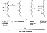 The logic N_P CMOS is used constituted from sections N-P
dominates having like escape stage one latch C2MOS, in such a way it optimizes speed and area.
In making that is necessary however to respect the following
rules:
to) every door C2MOS must be separated from the previous one by means of an equal number of reversals
b) us dynamic stage separated from previous door C must be at least one2MOS from one equal number of reversals.

19) Clock to 2 is made:
The adoption of a clock to two is made overlapped does not concur to eliminate the problems of clock skew even if the two can equally be introduced in the case are made meet such various delays to make to overlap the clock and therefore to render the structure transparent.
The clock to two it is made can be generated or externally or locally however the outline to implement is always following:

The memory structures are equal to the structures of memory to a phase with the only difference that in place of clk and â?"clk has phi1 and phi2 , analogous for the logical structures.
20) Clock to 4 is made:
 |
A clock to 4 it is made concurs to implement logical dynamics that beyond to having a phase of one of appraisal precarica and, have also a phase of hold, that eliminates the charge-sharing during the phase of appraisal.
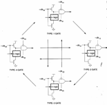 In order to avoid problems of charge-sharing the shapes of
wave of the clock can be altered forming an only one mark them of
clock from the sum of 2 mark them of clock. A such one I use of
clock the door to 4 various realizable logical structures di.le which
all the logons are not allowed but only those illustrating from the
following figure:
21) Criteria of chosen of clock and the its distribution:
It comes practically only used the clock to a phase in the how much simplest one to manage above all to growing of the demanded speed, the clock to two is made only finds application in RAMs, ROMs, PLAs.
As far as the distribution of the clock pu² to choose itself between the implementation of only buffer and a realization instead of a tree structure particularly adapted in the case the realized plan is characterized from one elevated modularity.
I/O Structures
22) Structures I/O:
They are the structures that demand a greater experience of the planner therefore often are preferred to adopt of the already present modules in the bookcases. In short there are of the pad of logon to the piedini whose dimensions are fixed from the resolution of the machine that executes the weldings and from the minimal dimensions necessary in order to knit a thread. Adjacent to the pad there are the circuits of I/O that can belong to the following categories:
to) Output pad
They are most subject to the latchup therefore makes appropriating I use of the guard-rings and fictitious collectors.
b) Input pad
 It must possess a protection for the gate ones of
the present MOS in income, it in kind is constituted from 2 diode
valves clamper that they limit the maximum excursion of the income
tension and from a resistance series that limits the peak currents
that they can slide in the diode valves, its value is comprised
between 200W and 3KW.
c) Pad tristate and bidirectional
A pad tristate it has the following outline

 while a pad bidirectional it is obtained from the
union of a pad tristate and of a pad of income
23) Plan in low power:
The plan in low power is based on uses only locally of the CMOS to tensions reduced totally or also where elevated speeds are not demanded, moreover work to low frequencies (…if not rerunning itself to the parallelizzazione) and is necessary to render the how much short possible line of clock in how much remains active also during the power-down.
