Characterization of the circuits and estimates of the performances
1) Esteem of the resistance:
The resistance introduced from a layer of material
conductor is  where Rs is the resistance of the sheet and measure in W/ .
Such resistances in the case of the polisilicio and the spreads
are influenced from the drugging concentrations of and the presence of
materials like the silicidi.
where Rs is the resistance of the sheet and measure in W/ .
Such resistances in the case of the polisilicio and the spreads
are influenced from the drugging concentrations of and the presence of
materials like the silicidi.
A device MOS moreover can often be characterized from its
resistance ![]() .
.
2) Condenser CMOS:
Condenser CMOS is formed exclusively from substrate p-doped, SiO2 and gate metallic or in polisilicio, can be introduced the following situations:
to) accumulation:
to the gate ones it comes applied a negative tension, it attracts gaps
to oxide therefore the ability is only that one of the  oxide with To = area of gate and andthe SiO2 = 3.9.
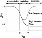 b) depletion :
a weakly positive tension removes gaps but it
is not in a position to attracting electrons, of it it derives that in
the pressed ones of oxide one is had emptied layer of bearers wide d
and having ability
b) depletion :
a weakly positive tension removes gaps but it
is not in a position to attracting electrons, of it it derives that in
the pressed ones of oxide one is had emptied layer of bearers wide d
and having ability  with and = 12.
 ![]() is therefore the capacità total introduced from the
condenser MOS, series of C0 and Cdep
is therefore the capacità total introduced from the
condenser MOS, series of C0 and Cdep
c) inversione : a advanced positive tension to the Vt recalls electrons from the substrate which come to constitute a channel, such electrons but do not succeed to follow variations of mark them of income to advanced frequencies to 100Hz therefore for inferior frequencies the ability are C0 while for advanced frequencies it will be necessary to consider also ability Cdep and therefore the total ability is Cgb that it is also the possible minim.
3) gate Abilities to to a MOS:
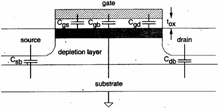 The parasitic abilities presents in a MOS are represented
from the following figure
The parasitic abilities presents in a MOS are represented
from the following figure
In particular the ability to the gate ones is Cg = Cgb Cgs Cgd where Cgs and Cgd are understandings between the gate ones and the channel therefore if this last one is absent is absent also they therefore to second of the region of operation of the MOS is had:
to) interdiction : the channel is absent therefore the only ability is givenC gb from the series of 0C and Cdep
b) non-saturazione :
the channel is formed therefore Cgb = 0 while ![]()
c) saturazione :
the channel is not formed from the side of drain
therefore Cgd = 0 while ![]()
To the aim to calculate the delays in the digital circuits them C g =C 0 canbe approximated .
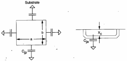 As far as instead abilities Cdb and Csb introduced
towards the substrate from the spreads of source and drain, is had
that ciascuna of it it is worth
As far as instead abilities Cdb and Csb introduced
towards the substrate from the spreads of source and drain, is had
that ciascuna of it it is worth ![]() where Cja is the vertical ability in between the
spread and the substrate while Cjp is the introduced peripheral ability from 4 sides of the
spread which has one not null depth.
where Cja is the vertical ability in between the
spread and the substrate while Cjp is the introduced peripheral ability from 4 sides of the
spread which has one not null depth.
It is Cja that Cjp is but function of the present
tension to the heads of the splice second  the
where Cj0 is the ability in the
case the tension to the heads of the splice is null, Vb @ 0.6V and m vary
from 0.3 to 0.5 to second of the discontinuity of the splice.
the
where Cj0 is the ability in the
case the tension to the heads of the splice is null, Vb @ 0.6V and m vary
from 0.3 to 0.5 to second of the discontinuity of the splice.
4) Analysis and solutions for distributed circuits RC:
In the case of logons in polisilicio many long or logons
in metal heavy loaded, are had of the forts delay of propagation that
can be study by means of the theory of the lines thinking the line to
you subdivided in infinite having drafts infinitesimal thickness,
resistance to length unit r and ability to unit of length c, derive
that endured delayt x from
one marks them that a discreet analysis crosses a distance along ![]() x è door instead calculating the due delayt n to the section n-esima,
has
x è door instead calculating the due delayt n to the section n-esima,
has  .
.
The quadratic course of the delay regarding the distance is much heavy one, much to render advisable in some cases to insert of the buffer along the line which regenerate mark them, the delay that is obtained also considering an inner delay to the buffer of some ns, is always inferior to the delay that is had in absence of the buffer. Alternatively the source in chip so that it tos be distant little from the adressee, the this can be decided is the reason for which the clock sovente it is found to the center of the chip. A model for the calculation of the delay is:
5) regarding characteristic Times the commutation of one door:
tr necessary time so that the escape passes from 10% to 90% of its stationary value
tf necessary time so that the escape passes from 90% to 10% of its stationary value
td time that elapses between the variation of 50% of the income and the variation of 50% of the escape, comes also defined the times tdr and tdf relati you to the increase and the reduction
6) analytical Model of delay of inverter a CMOS:
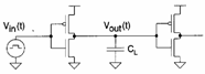
 They come calculates the t to your and tf for
the following circuit when it is to it applied to a wave quadrant with
foreheads to infinite slope. For the calculation of the time of
reduction, we make reference the nMOS. If in income there is 0
then the nMOS it is interdetto (X1) and the escape will be to the
maximum value VDD . When
the income passes to 1, the nMOS instantaneously it passes in
saturation (X2) and begins to unload a rampa second, but when DD
arrives toV out =V â " Vtn it passes in saturation and discharge
with quadratic law until Vto SS (X3).
They come calculates the t to your and tf for
the following circuit when it is to it applied to a wave quadrant with
foreheads to infinite slope. For the calculation of the time of
reduction, we make reference the nMOS. If in income there is 0
then the nMOS it is interdetto (X1) and the escape will be to the
maximum value VDD . When
the income passes to 1, the nMOS instantaneously it passes in
saturation (X2) and begins to unload a rampa second, but when DD
arrives toV out =V â " Vtn it passes in saturation and discharge
with quadratic law until Vto SS (X3).
Evidently therefore the calculation of the time of
reduction is subdivided in two is made, in which the nMOS it is in
saturation (…is resolved for separation of variable the
![]() equation, integrating between 0.9VDD and VDD- Vtn
equation, integrating between 0.9VDD and VDD- Vtn ![]() …is obtained) and the other in which it is
in region of triodo
…is obtained) and the other in which it is
in region of triodo
(…with the expression ofthe DS for the region of triodo and
integrating between VDD â "
Vtn and 0.1VDD is obtained ![]() … ). The sum of the two times can be approximated to
comprised
… ). The sum of the two times can be approximated to
comprised  the value with k between 3 and 4 and
in analogous way that is obtained for the time of
the value with k between 3 and 4 and
in analogous way that is obtained for the time of  climb, implies that if the MOS have the same dimensions,
the time of climb is the double quantity of the time of reduction in
how much mobility of electrons is double regarding mobility of gaps,
for having the same times is necessary to make Wp = 2 Wn .
climb, implies that if the MOS have the same dimensions,
the time of climb is the double quantity of the time of reduction in
how much mobility of electrons is double regarding mobility of gaps,
for having the same times is necessary to make Wp = 2 Wn .
As far as the times of delay they are simply the half of
respect times to you of climb or reduction and can be expressed in the
shape ![]() e
e ![]() where Top andn they have a complex expression but
they can be approximates you to calculated value 0,36 with SPICE.
where Top andn they have a complex expression but
they can be approximates you to calculated value 0,36 with SPICE.
7) Delay of one logical door:
The delay of simple a logical door can be calculated constructing inverter an equivalent in which that is the dimensions of pull-down and the those of the pull-up reflect the distances that effectively are active in the pull-down and in
 pull-up, in particular considering as an example
one nand to 3 incomes
pull-up, in particular considering as an example
one nand to 3 incomes
it is had that for the pull-down it is necessary
to consider the series of the 3 nMOS and therefore of their
conductances therefore for bn1 = bn2 = bn3 ![]() is had while for the pull-up
it is necessary to consider only 1 pMOS therefore
is had while for the pull-up
it is necessary to consider only 1 pMOS therefore ![]() after all considering
after all considering ![]() e
e
![]() ha tr @ tf . This methodology can be motivated
imagining to make to stretch to 0 the distance between the gate ones
of the 3 nMOS, has in fact in such only case gate a wide one 3L.
ha tr @ tf . This methodology can be motivated
imagining to make to stretch to 0 the distance between the gate ones
of the 3 nMOS, has in fact in such only case gate a wide one 3L.
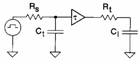
8) Infuence of the slope of the shape of wave of income on the delay of one logical door:
The slope of the shape of income wave can modify the delay
of a door, in particular if the foreheads are the much steep then
delay are determined mostly from the distances of load and unload
while if the varied income slowly then contributes to the delay of the
escape, in particular  is had where tdr-step it is the time of delay in climb
that is had for an income to step, tinput-fall is the time of reduction of the income and
is had where tdr-step it is the time of delay in climb
that is had for an income to step, tinput-fall is the time of reduction of the income and ![]() .
.
In analogous way  con
con ![]() is had.
is had.
9) Models switch in order to calculate the delay of one door:
They are models for the calculation of delays of complex doors, the MOS like resistances that they load and they unload of the abilities, in the fattispecie are based on considering are assert following the 3 models to you:
to) RC
 where Rpull-down is the resistance total met in
the distance of pull-down while Cpull-down the relative abilities to the nodes been involved in the
commutations are all. In analogous way it is estimated tdr .
where Rpull-down is the resistance total met in
the distance of pull-down while Cpull-down the relative abilities to the nodes been involved in the
commutations are all. In analogous way it is estimated tdr .
b) Penfield-Rubenstein
 where R is
the resistance from the node back VSS if the fall-Time is considered (…or towards VDD if the laugh-Time is
considered) while C is the ability to
node i.
where R is
the resistance from the node back VSS if the fall-Time is considered (…or towards VDD if the laugh-Time is
considered) while C is the ability to
node i.
c) Slope
It defines the intrinsic time of climb like the time of climb that would be had if in income came applied a step. The time of effective climb comes subdivided for the intrinsic time of climb.
d) Penfield-Rubenstein Slope Delay
Combination of the Slope and the Penfield-Rubenstein is one.
10) Model in order to calculate the delay of circuits many complexes:
The delay of one given door comes determined by means of a
simulator from which an equation of the type ![]() is obtained where tinternal it is an introduced fixed delay from the door while toutput it is a delay proporziona
them to the cargo k.
is obtained where tinternal it is an introduced fixed delay from the door while toutput it is a delay proporziona
them to the cargo k.
11) Body â " effect in the delays of the logical doors:
NMOS the more neighbors to the escape of a door nand have V sba ¹ necessarily 0, that ago that they are more discs of a valve in the commutations effect that becomes obvious if the escape ability is comparabile to the inner abilities.
We consider the two following doors nand:
the nand up he has all the nMOS ignited except that one up, of it he derives that its source is to mass and therefore when the income passes to 1 the escape commuta quickly to 0. In nand low instead all the nMOS up they are active while that one low is initially interdetto, follows some that the abilities will be all charges to the high level and when the income high-pass filter, will have to be unloaded all before in order to low concur the commutation of the escape from the high level with the level that therefore happens in a time longer than how much is not had up for the nand.
In order to diminish the effects of the body â " effect the following strategies can be used:
to) diminishing the abilities to the inner nodes
b) to place the having MOS it marks them that they arrive for last more close possible to the escape
12) Dimensioning of the transistors in doors CMOS:
In kind W p= 2 is made Wn so as to to equalizzare the times of it loads and discharge, but in such a way is had an increase of the occupied area and the dynamics dissipation therefore when possible the following strategies are applied:
to) a brace of inverter places in having series withW p = 2W n from place to the same delay generated from a brace of inverter Wp = Wn , in order to demonstrate it is R and Ceq respective the resistance and the ability equivalent of a having MOS unitary dimensions, and considers the following delays for configurations:
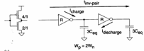 The ability is 3Ceq in how much is the parallel of the ability to the nMOS that
it is worth Ceq and of the
ability to the pMOS that is 2Ceq in how much Wp = 2Wn , of it it derives that the
time of reduction is
The ability is 3Ceq in how much is the parallel of the ability to the nMOS that
it is worth Ceq and of the
ability to the pMOS that is 2Ceq in how much Wp = 2Wn , of it it derives that the
time of reduction is ![]() while the time of climb is
while the time of climb is ![]() in how much the pMOS having Wp = 2Wn has resistance halved regarding the nMOS minimum-size,
therefore totally the delay is
in how much the pMOS having Wp = 2Wn has resistance halved regarding the nMOS minimum-size,
therefore totally the delay is ![]() .
.

Being Wp = 2Wn the ability to the nMOS is
equal to that one of the pMOS therefore will be had 2Ceq , of it derives that the time of
reduction is ![]() while the time of climb is
while the time of climb is ![]() in how much the pMOS having Wp = Wn has
resistance halved regarding the nMOS minimum-size, therefore totally
the delay is
in how much the pMOS having Wp = Wn has
resistance halved regarding the nMOS minimum-size, therefore totally
the delay is ![]() found that is the same one for
the other configuration, with the difference that in this last one
comes diminished the area in how much has Wp = Wn ,
naturally this change of W influences b and consequently also the Vinv which but can vary to the maximum of 15%.
found that is the same one for
the other configuration, with the difference that in this last one
comes diminished the area in how much has Wp = Wn ,
naturally this change of W influences b and consequently also the Vinv which but can vary to the maximum of 15%.
b) In order to pilot cargos a lot elevates to you can be inserted of the inverter in cascade of gradually increasing dimensions in way but to diminish the delay, the area and the dissipation.
![]()
It is to the increase percentage of the dimensions of a
inverter regarding the previous one and td the introduced medium delay from inverter to minimal
dimensions, then a delay introduced from every stage is atd while the delay total is natd that if we place  it becomes
  where the fractional amount is the
only one on which it can be taken part, is had that it is minimal for
to = and @ 2.7 however in kind
in the applications can to have been comprised between 2 and 10.
where the fractional amount is the
only one on which it can be taken part, is had that it is minimal for
to = and @ 2.7 however in kind
in the applications can to have been comprised between 2 and 10.
13) Power dissipated from a circuit CMOS:
![]()
to)  Ps it has had to the static dissipation that in the case of
the CMOS is exclusively due to the diode valves adorned to you
inversely polarizes you for everyone of which has
Ps it has had to the static dissipation that in the case of
the CMOS is exclusively due to the diode valves adorned to you
inversely polarizes you for everyone of which has  and therefore considering n dispositi to you, the
dissipated static power is
and therefore considering n dispositi to you, the
dissipated static power is  , for a typical one
inverter fed to 5V has Ps @ 1nW.
, for a typical one
inverter fed to 5V has Ps @ 1nW.
b) Pd is the dynamics power dissipated in order to load and to
unload the cargo ability, considering in income a having wave ideal
quadrant period tp has  .
.
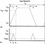
c) Psc is the power dissipated in short circuit when the income is
not a wave ideal quadrant but more really it is introduced like a
repetition of trapezes like evidenced in figure, has ![]() with
with  ,
, ![]() is obtained where trf it is the
time of climb or reduction of the shape of income wave and can give
place to variations of 20% in the case of inverter loaded.
is obtained where trf it is the
time of climb or reduction of the shape of income wave and can give
place to variations of 20% in the case of inverter loaded.
The calculation of the dissipated power must be carried out for every ability to the frequency for which it is operating.
14) Charge - sharing:
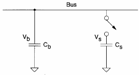 When a bus characterized from one ability C b
witha device characterized from one is wanted to be sampled ability Cs must be made so that the
tension Vread R is almost
equal to present tensionV b
on the bus, in particular before the closing of the switch Q
b=C bVband also Q s=C
sVs is had while after the closing
When a bus characterized from one ability C b
witha device characterized from one is wanted to be sampled ability Cs must be made so that the
tension Vread R is almost
equal to present tensionV b
on the bus, in particular before the closing of the switch Q
b=C bVband also Q s=C
sVs is had while after the closing ![]() is had that in case Vb= VDD>> Vs is reduced to
is had that in case Vb= VDD>> Vs is reduced to  that therefore respects the single condition if Cb>> Cs, in the applications has Cb> 10Cs .
We consider hour a static door nand to 2 incomes initially both
to 0 and therefore the escape is to 1, when the nMOS up the escape
passes to 1 must still be 1 however for charge sharing is lowered
regarding VDD in how much is
the ability parasite mails between the two MOS.
that therefore respects the single condition if Cb>> Cs, in the applications has Cb> 10Cs .
We consider hour a static door nand to 2 incomes initially both
to 0 and therefore the escape is to 1, when the nMOS up the escape
passes to 1 must still be 1 however for charge sharing is lowered
regarding VDD in how much is
the ability parasite mails between the two MOS.
15) Yield of a wafer:
Draft of the relationship between the n° of chip good presents on wafer and n° a total of chip present on the same one, it is function of the area To of the chip and of the density of D defects, the following models are had:
to) Seed ![]() it is a model used for chip much large having one
rendered inferior to 30%
it is a model used for chip much large having one
rendered inferior to 30%
b) Murphy  is a model used for chip small with advanced yields to 30%.
The yield can be increased increasing the redundancy of the circuits.
