Technology of processes CMOS
1) Wafer:
Draft of a having silicon disc diameter comprised between 7,5cm and 23cm and inferior thickness to 1mm, is obtained slicing with a diamond blade a silicon ingot to single crystal that in its turn is obtained with the Czochralski method. In particular a silicon fusion is had policristallino that it comes scaldata in a crucible by means of radio frequency, the fused one comes maintained to 1425°C that is to little advanced temperature to that one of fusion of the silicon, comes in it dipped a silicon crystal that determines the direction of the obtained ingot, it comes then ruotato and extracted generating the ingot with rhythms of increase between 3cm/h and the 18cm/h.
2) Methods of oxidation of the wafer:
The oxidation of the wafer happens heating them in an oxidating atmosphere, in particular is had:
to) Dry Oxidation: the atmosphere contains only oxygen, of it derives a slow process for velocizzare which temperatures of approximately 1200°C are used.
b) Wet Oxidation: the atmosphere contains vapor of water, a process derives some express for which a temperature comprised between 900°C is sufficient and 1000°C.però an oxide of insufficient quality is obtained.
The obtained oxide has a volume approximately double quantity regarding the volume of the consumed silicon and it fairly expands in both the vertical directions.
3) Realization of zones with various concentrations of impurità:
to) Epitassia : comes grown a film monocrystal subjecting the wafer to elevated temperatures and una drogaggio source.
b) Deposizione : comes evaporated a material drugging on the surface of the silicon, to follow has a thermal cycle that diffuses the impurità in the bulk
c) Impiantazione: the surface del silicon comes bombed with donori atoms or having accepters elevated energy, to advanced temperatures to 800°C has the spread delle impurità between various having zones density.
4) selective Spread:
The ability to act agrees from barrier in the dopanti comparisons of the impurità introduced from some materials which:
to) fotoresist
b) polisilicio
c) silicon dioxide SiO2
d) Nitrate of silicio SiN
They in particular come use you in order to realize of the masks that concur the selective spread.
5) Removal of oxide:
The oxide comes covered from the fotoresist, to it it comes overlapped a mask in the zones where it desires that the oxide remains (…fotoresist positive), such mask protegge the fotoresist below from beams UV and therefore it does not polymerize, what that instead happens for the fotoresist not masked, which can be removed with an organic dissolvent, the opened window therefore concurs the elimination of below oxide by means of an acid with which instead the fotoresist resists.
6) EBL:
The technique of the masks concurs unfortunately to realize lines of equal minimal amplitude to0,8m m while the Electrom Beam concurs to arrive to0,5m m, draft of one technical much precise and with many advantages but also much expensive one.
7) Polisilicio:
The polisilicio is a structure in not monocrystalline silicon that is obtained depositing on SiO2 , draft of a material that is behaved from screen in the comparisons of the spreads of impurità and therefore it comes mainly used in place of the metal in order to realize the gate ones of the MOS with the aim to maintain therefore separates to you source and drain, moreover the drogaggio of it reduces the resistance to values many bottoms. Drugged Polisilicio does not come instead used in order to realize resistances much high one in the static memories.
8) Process nMOS:
to) by means of the active mask SiO 2 from the region is eliminated where the nMOS is wanted to be realized
b) the oxide fine or oxide is deposited of gate having one thickness of approximately 100Å
c) deposits the polisilicio that goes to form the gate ones
d) the gate oxide is eliminated of from the regions where for impiantazione they are come true then of deep spreadsn approximately 1mm and relative to the source and the drain
and) an oxide is often deposited and subsequently the metallic contacts to the source and the drain are come true
9) Typology realizzative CMOS:
to) process n-well
b) process p-well
c) Twin-Tub process
d) process SOI
10) Process CMOS n-well:
to) it comes realized the trap n destined to accommodate the pMOS
b) by means of the active mask they deposit 2SiO and SiN in the regions where the MOS are wanted to be realized
c) the substrate p comes drugged p in the external zone to that it will accommodate the nMOS and that it is covered from SiN
d) it often comes grown oxide in the zones where not there is SiN, however it grows is vertically that laterally giving place to a shape to bird spout that reduces the active region but it renders the structure flat
and) Introducing a loaded layer negatively to the interface oxide-silicon the tension of threshold V can be changedt is of the pMOS that of the nMOS
f) the oxide of gate is deposited and the polisilicio to U in how much must connect the two gate ones
g) They come carried out spreads n of nMOS and p of the pMOS
h) They come realizes the contacts, the metalization and the passivazione to you.
i) the substrate that accommodates the nMOS comes connected to VSS while the n-well that it accommodates the pMOS it comes connected to VDD .
11) Characteristics of process CMOS p-well:
The realization is complementary to that one of the CMOS n-well however considering that the transistor realized in the substrate has better property and that the pMOS they have inferior gain regarding the nMOS, of it derives that if a CMOS with nMOS is desired and pMOS with balanced characteristics the how much most possible one convene to resort to a process CMOS p-well.
12) Twin-Tub Process:
A epitassiale layer separates substrate n from the overhanging region where they are realized is the n-well for the pMOS that the p-well for the nMOS, in such a way the latchup is prevented and MOS with balanced characteristics are obtained.
13) SOI:
With the aim to reduce the effects of the latchup and to increase the speed, the technology Silicon On Insulator has been developed where the insulator is in kind zaffiro.
14) Improvements of technology CMOS:
with) added the more levels than metal (…in kind connected layers of aluminum between they by means of VIA) and of polisilicio a better shunting of the feedings concurs and of it marks them let alone in particular of the clock
b) the resistance of the polisilicio used for the gate ones is of approximately 30W/ , that can give place to delays consisting in the case of long lines, therefore it is preferred to use silicide that is polisilicio/tantalio or an overlapped layer of silicide to a layer of silicide, in such a way the 3 resistance of the gate ones is reduced toW/.
15) BiCMOS:
Draft of a process in which they are present transistors npn, pnp, nMOS, pMOS, it is used particularly laddove must be piloted great cargos and is demands low times of delay, this is as an example the case of the memories and the given buses of mthe processori.
16) Design rules:
Draft of rules times to obtain the principle rendered in the minimal possible area, to such aim places geometric restrictions on the masks and the interactions between the different layers, they can be expressed in the two following form to you:
to) Micron-rules
b) l- based-rules they cannot be used under the mm
17) Some designs rules for processes CMOS:
to) the polisilicio this to the aim must be extended beyond the region of the spreads to avoid contacts between source and drain
b) the guard rings they prevent the latchup, in particular draft of spreads p nel substrate p which are come connected to VSS or of spreads n nel substrate n which come connected to VDD .
18) Origin and development of the latchup:
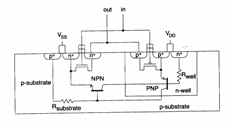
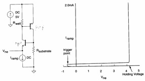
The latchup it is a phenomenon that in past has prevented the development of technology CMOS, draft in fact of a circuit parasite inborn in process CMOS which under opportune conditions door to the short circuit between VDD and VSS with consequent damage of device CMOS, all that it is reassumed from the following figure:
 |
 |
||
In short if current in the emettitore of the npn slides one, it is come to having that its VBE = 0,7V therefore passes in conduction and therefore will slide current also in the emettitore, of the rest the fall on RWell determines Va BE = -0,7V for the pnp that therefore it in conduction passes also therefore ulteriorly slides current inR Substrate and therefore npn the door towards the saturation, this hard rigenerativo effect sinchè does not catch up the trigger-point, beyond which it is in one be stable that door until to the holdingones for which the short circuit is had. The reasons that they can give place to the latchup are therefore essentially extracurrents which those that they can be introduced in the I/O circuits.
19) Methods of prevention of the latchup:
to) the b can be reduced of the two transistors adorned to you
b) the values of the resistances R Well and Rcan be reducedSubstrate
c) can be inserted of the guard rings which they act like fictitious collectors who absorb the minority bearers lowering therefore the gain of the npn and of the pnp.
d) much drug addict can itself be made a substrate and to cover it with a epitassiale layer, in such a way reduces the value of the resistance of the substrate
and) the R Well by means of onecan be reduced layer leggermente drug addict overlapped to one layer heavy drugged.
