Charge Coupled Device
1) historical Introduction
5) Imaging CCD
5b) Architectures
5c) Rooms to colors
Course of ELECTRONIC DEVICES
Academic Year 1999/2000
Antonio D' Ottavio
1) historical Introduction
The first CCD has been developed in the laboratories Bell di Murray Hill, New Jersey in the 1969 from the investigators Bill Boyle and George Smith, they were engage to you in the search of new methods for the acquisition of images with the aim to realize the Picture Phone, they knew perfectly therefore is the possibility to store loaded electrical worker by means of a condenser MOS that the technology of the memories to magnetic bubbles, from connubio of these the two acquaintances nacque the idea to group the dominions of I accumulate of the charges and to use opportune potential differences them electrical worker in order to transport them from a dominion to the other. Draft therefore of a device conceptually simple a lot that the criteria base were adopts a position to you in little hours and the first prototype to 6 pixel was ready after sun 6 weeks, perhaps just in this semplicità and in the myriad of possible applications the reason of its succeeded one that resides the door to being one of the devices electronic you that guides the technological development puts into effect them.
Like pointed out in the introduction, a CCD is not other that with with disposed condensers MOS many neighbors between of they so that applying an opportune polarization it can be transferred loads present in one of they in an other to adjacent it, the structure of every condenser MOS is therefore following:

A silicon oxide is had SiO2 that separates of the P-doped silicon from a metal (…in kind aluminum) that it constitutes the electrode (…called Gate) to which comes applied the polarization necessary to create the emptying region whose extension comes limited through the two channels of stop that they come realizes to you by means of of drugged zones p .
The modalities of creation of the region of emptying in function of the tension applied to the Gate demand an analysis of the system in terms of energy bands, it come therefore developed for following arrange in which for semplicità they have been neglects the two channels to you of stop:

we consider for this system loads accumulated to the splice oxide-semiconductor, the ability and the bands of energy in the case are not polarized or polarized in the regions of Depletion, Reversal and Accumulation.
to) Zero Bias (Depletion)
Once that the materials are connected to form an only system has an electron flow from the metal to the semiconductor through a whichever circuit that present a smaller resistance of that one introduced from oxide, in this way on the metal has a sheet of loads positive while the electrons that reach in the P-doped neutralize part of gaps creating a region of emptying in the pressed ones of oxide, in it present only Ionian is denied to you, it follows some that in this region the valence band goes away from the level of Firm andf .
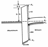
One important descriptive characteristic of the system
is upgrades them superficial ![]() where and(0) it is the Firm energy of the situated
level of intrinsic to half of the Gap, in particular embezzling to it
upgrades them superficial upgrades them fp that we have in the bulk we obtain
the fall of upgrades them to the heads of the region of Depletion.
where and(0) it is the Firm energy of the situated
level of intrinsic to half of the Gap, in particular embezzling to it
upgrades them superficial upgrades them fp that we have in the bulk we obtain
the fall of upgrades them to the heads of the region of Depletion.
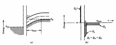
 Applying tension positive on Gate not makes other that
to strengthen this situation in fact other gaps will come recalled
towards the ohmmico contact and therefore the extension of the region
of Depletion will increase, moreover band of valence will remove
ulteriorly from andf until to
reach condition limit in which andf = and in correspondence
of which the bands and the distribution of load they are those
illustrating in figure. The ability introduced from the system
is equal to the series of the ability to the
 ![]() oxide and of the ability associated to the region of
Depletion
oxide and of the ability associated to the region of
Depletion ![]() therefore it decreases to growing of
xd that is to growing of VG .
therefore it decreases to growing of
xd that is to growing of VG .
C) Reversal
 When
When
In order to estimate the system capacity MOS when it is
polarized in reversal region it is necessary to hold account of the
rapidity with which they vary
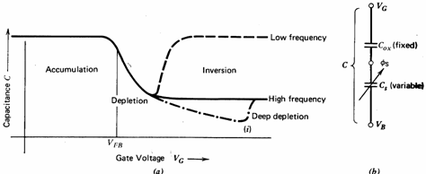
Low Frequency both the tensions vary to an inferior frequency ai 10Hz , that concurs ai bearers generates you to follow the variations della loads sul gate and therefore the associate ability is only that relative on the credit side oxide.
High Frequency Vvaried G to one inferior frequency to 10Hz the while vg it varies to one advanced frequency, of it follows that the bearers generate to you do not succeed to follow the variations of load on the gate ones and therefore the associate ability is that relative one to oxide with in series the ability to the region of depletion, which stretches to a value limit when the system goes in Strong Inversion that is when it is had |fs| > |fp| and therefore the free electron concentration in surface is greater of the gap concentration in the bulk.
Deep Depletion both the tensions vary to a advanced frequency to the 10Hz , it follows some that the layer invert does not succeed to form itself and therefore the region of Depletion extends beyond the maximum value that is had in Strong Invertion, follows some that the ability total of the system decreases ulteriorly, however to growing of Vthe G increases the extension of the region of Depletion and therefore it increases also the generation of bearers and a collassamento of the ability is had on the value that assumes in the case of High Frequency.
Curve C-VG that reassumes the previous considerations is therefore following:
 |
 |
For thoroughness of used analysis seppur in the CCD it does not come also described the accumulation region that is had when the Gate with an inferior tension to V FB =f M is polarized - fs , is had that they come recalled from bulk the other gaps which are gotten thicker in the next region to oxide, the bands in bulk of the traslano semiconductor towards the bottom and therefore the band of valence is approached to andf .
The ability associated to system MOS is in this case only Cox .
Based on how much approval on condenser MOS it is had that for advanced tensions of Gate to the threshold tension, it can be loaded to a whichever value comprised between Qn= 0 correspondent to the operation in Deep Depletion and the value with Qn correspondent to the operation in Reversal.
In the Imaging-CCD instead the condenser it is found in region of Depletion and the photons incidents generate load piece of furniture in how much hitting produce of the braces electron-gap.
Independently from the way in which it loads comes generated, the more important functionality of the CCD is sure the transfer of the same one that is based on the application to the Gate of tensions that generate opportune holes of upgrade them in which it loads remains caught until to the successive transfer, considers the operation of a CCD to 3 is made which that illustrating in figure:

it is constituted from 3 condensers MOS places side by side to you, in storage mode the charges comes stored under the electrode centers them where a more positive tension regarding those applied to the adjacent electrodes creates a hole of upgrades them.
In order to transfer the package of it loads stored in the condenser centers them in the condenser to its right, is necessary to apply to its Gate a more positive tension so that the charges migrino towards the region where it upgrades them are lower.
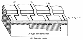
After that the transfer of loads from an electrode to other has happened can be brought back both the tensions to inferior values, so as to to concur with the same tensions a successive transfer.
An inferior limit to the speed exists with which it loads must be transferred from a condenser MOS to the successive one, in particular such limit is dictated avoiding that it loads thermally generated saturates the channel, this happens in some second ones however is not a problem in how much in the applications is attempted to approach itself the advanced limit, desires in fact of the faster registries to sliding how much possible one. The maximum frequency that currently can be applied to a CCD is of approximately 30MHz, this because an other fundamental requirement must be guaranteed that is that all loads comes transferred from a CCD to the successive one.
Can therefore be realized registries to sliding are
analogic that digita them, in particular in the digital applications
them it is made to correspond a â?

Part, as an example, from a â?

Wanting to carry out a transfer towards right we apply one tension V3 to electrodes 2, 5, 8 loads present in electrodes 1, 4, 7 is moved under of they.
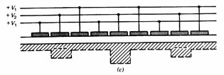
Finally once happened the transfer we bring back the tensions to lower values.
V are observed thatV 2 characterize always the MOS where load currently memorizzata,3 characterize the MOS where load will have to be transferred to the successive step and V1 characterize the MOS that acts as from separator towards an other element CCD.
4) Evolution of the CCD: the Buried Channel CCD
The greater limitation of the traditional CCD is the presence of superficial states trap, these absorbs the minority bearers preventing of an effective transfer that it above all reveals deleterious in matrices CCD many extending. The problem comes resolved using a superficial channel but a channel buried like in the not following structure:
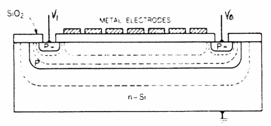 |
draft of a CCD P-Channel to 3 is made, constituted from a N_doped substrate on which a concentration of the accepters is realized having the P-doped channel 20 times greater of the concentration of the donori in the N-doped, such layer is often some mm and is connected to its ends with contacts p and moreover it is sormontato from 2SiO and metallic electrodes.
To the escape diode valve it comes applied one such tensionV 0 to empty the buried channel of majority bearers, the order of magnitude for this tension can be found from the course of upgrades upgrades them them in function of the distance from the interface â " SiO2 :
it can be observed that a minimum is had of upgrades them for gaps just in correspondence of the buried layer, its value is of â?"37V.
It comes illustrated the course is in the presence case
that of absence of it loads in the channel, and as indicated the
ability to the structure it is of approximately ![]()
 while per a traditional CCD it
is
 ![]() . This inferior ability is one of the
main disadvantages of the Buried Channel CCD regarding the traditional
CCD however has the advantage that the transport is entrusted the
majority bearers and therefore it does not happen for spread but for
drift, moreover mobility in the bulk is approximately the double
quantity of that it is had in surface.
. This inferior ability is one of the
main disadvantages of the Buried Channel CCD regarding the traditional
CCD however has the advantage that the transport is entrusted the
majority bearers and therefore it does not happen for spread but for
drift, moreover mobility in the bulk is approximately the double
quantity of that it is had in surface.
One of the characteristics more important than a CCD is
the distance between the electrodes, it in fact gives place to of the
fields of fringe which a course corresponds of upgrades them various
from that one wished, as an example for a Buried having Channel 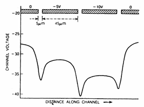 CCD a distance between the electrodes of 5mm in correspondence of the
space comprised between two electrodes has itself of the bags of
upgrades them which are in a position to absorbing loaded that instead
the successive electrode would have to be transferred from the below
region a data electrode to the below region, all that goes to
discapito of the efficiency of the transfer of loads and therefore he
is not acceptable especially in the matriciali CCD in which it
loads must endure a high number of transfers.
The way more obvious than to reduce the bags of upgrades them is that one to reduce the distance between the electrodes, the result that obtains in a case limit making to stretch to zero such distance has been calculated numerically and brought back in the following figure:
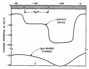
the absence of bags is obvious of upgrades them is in a superficial CCD that in a Buried Channel CCD moreover from the figure is important to find that in the below space the electrode upgrades them of the Buried Channel possesses a slope much greater one of the superficial CCD that numerically it means a greater electric field 10 times and therefore a greater speed in the transfer of the charges that has carried the Buried Channel to being employed mostly in the applications in which one elevated frequency of clock is demanded, the limit which MHz is joints is of approximately 30.
Naturally the distance between the electrodes cannot be carried to zero, and then they have been developed other techniques in order to reduce the bags of upgrades them between which that one that has given the best ones turns out to you is the impiantazione of Boron atoms in the channel in correspondence of the spaces comprised between the electrodes.
The field that mainly has given the impulse to the search on the CCD is what it sees it used like optical sensor, innumerevoli applications are in fact possible are as far as the field of the visible one and therefore automatic control systems to us that for that regards astronomy, this last one in particular has been completely rivoluzionata from the advent of the CCD which possess clearly advanced characteristics regarding the other sensors use you previously. For a reason or purpose of example the equipment of the Advanced is introduced Room for Survey (ACS) installed to edge of the Telescope Spaces them Hubble, it is composed from three photometric rooms, before, the "Wide Field Room" WFC, micron uses two CCD thinned back-illuminated from 2048 x 4096 pixel (pixel size = 15) realizes to you from the Situated ones that come mount to you to mosaic for a total of 4096 x 4096 pixel, comes used for the observations in v bands and I.
micron) that special treatment has one in order to obtain high sensibility in spectral range 200 -
400 nm, it is used for the observations to high resolution in band 200 - 1000 nm.
spectral range 150 - 170 nm. It makes use of a detector to "conteggio of photons" called Fines
Anode Microchannel Array (MAMA) formed from Micro a Channel Plate (MCP) to channels curves
with a fotocatodo to the Ioduro di Cesio (CsI) and from an able fine-electrode anode to obtain
 |
an area of 1024 x 1024 pixel with every pixel from 25 micron, comes employed for observations in the band 150 - 200 nm.
The successive paragraph means to describe some of the detailed lists and the constructive technologies that have carried to the choice of this particular equipment.
5a) Characteristic technical of the CCD
Geometry
The parameters more important consider you to care of geometry of the CCD are the dimensions of the pixel and the sensitive area constituted from the matrix CCD, particular applications demands a wide sensitive area but this goes to discapito of the scansion speed, some sensors and the characteristic correspondents are introduce to you in the following table
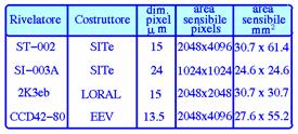
He observes myself that all these CCD are of the Buttable type that is can be composed nearly to form a mosaic in the case are demanded one greater sensitive area of that blanket from everyone of they.
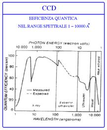
Quantica efficiency
Draft of the relationship between the photon number incidents on pixel and a number of braces electron-gap generated in average in a second, is a smaller number of 1 that comes expressed in percentage and is function of the wavelength of the photon incident, typically for a CCD has the following course:
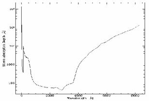 |
 The motivation of this curve is from searching itself in
the depth of absorption of the used Silicon in order to realize the
CCD, for it is had:
It is necessary in fact to confront this depth of penetration with the useful thickness to the aim of the photoelectric effect of the CCD, this is gone around around to i 15mm, have i remarkable cases:
to) 
 a photon UV that rilascia its
energy to a depth of 30 ..., generates it loads just on the
electrode. In this case, it loads comes lost because it enters
in the circuit like current.
b) For a blue photon the depth is of 0.2 micron, and therefore such photon can generate the brace and gap just under the electrode
c)  For a red photon or of
the close-infrared, instead, the depth of absorption is such to
generate loads in a useful zone for being able to be collection.
As saying the answer of sensors CCD in the ultraviolet one is of all the unsatisfactory one therefore they have been affinate following the two techniques in order to improve it:
to) the sensitive surface it comes dealt with a phosphorescent material which it executes the shift of frequency from the ultraviolet one to the visible one and therefore are worth the considerations on the absorption for it carried out.
b) the CCD comes lost weight and illuminated they give behind, in such a way eliminates the effect of the absorption from part of the electrodes, the defect is that in the thinning process a native oxide is created which forms a trap for the charges fotogenerate close to the sensitive region, the problem can be resolved implanting Boron atoms and proceeding to their annihilation, in such a way in fact other is not made that to fill up the trap.
A lost weight and illuminated CCD gives behind introduces exceptional a quantica efficiency regarding all the other devices uses you you before the advent of the evidenced CCD like from the seguente:
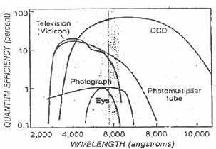
pack-saddles to observe that to 6000... the CCD he is 70 times more efficient of the photographic film, this wants to say that if to parity of conditions the time of integration with a CCD for a source weak person is of a minute, with a photographic film is 1 hour.
Current of buio
Also in photon absence incidents they are had
of the electrons that for thermal agitation pass from the band of
valence to the conduction band, this is never true how much for the
Silicon which it introduces a Gap of 1,1eV that as an example it means
that a pixel from 20mm to
It can be obviated to the problem embezzling to the image originates them an other image, dictates
dark frame, of the same obtained duration shielding the CCD, in this last one sara'
present the solo marks had them to the temperature that eliminera' therefore that present in the useful image. Affinchè this operation produces an optimal result is necessary that the duration of the dark frame is identical to that one of the image originates them and that the temperature of the not others CCD in the time that elapses between the two resumptions. In any case the current of buio can heavy be reduced making to work the CCD to inferior temperatures to the â?"100°C.
Efficiency of transfer (CTE)
It is the ability to transfer loads from a pixel to the successive one, is a parameter a lot important especially for large matrices CCD much in which before reaching the escape circuit the package of loads must cross many pixel, a reasonable value for the CCD puts into effect them is 0,999996 which it implies that for a matrix of 2048 x 2048 load found from the pixel more far away are reduced only of 2.5% during the transfer.
Uniformità
Illuminating a matrix CCD uniform we would want
that every pixel it stored the same charge, the causes for which that
it does not happen resides in the variation of the thickness produced
from the thinning techniques. Analogous to how much it is had
for the current of buio, the linearity can be eliminated not
illuminating uniform the CCD and acquiring an image Flat Field
dictates after which the acquired images come all standardized
dividendole for
Once that the image has been found from matrix CCD it is necessary to transfer it to the computer that elaborates it, the modalities of this transfer influence the speed of capture of the images, the architectures that have been asserted are:
Full Frame Transfer
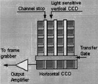
The photons incidents produce accumulate of load nelle vertical columns of CCD, al term della exposure the Gate Transfer qualify the passage del contained della line in realized horizontal bottom nello shift register with a shielded CCD, nel meantime all the other lines della matrix slide towards the bottom. A horizontal sliding of the packages is had then of loads towards the Output Amplifier which it sendes the information to the interface towards the computer. After that the last package of loads present in the horizontal CCD of it is exited, the Gate Transfer of it qualifies newly the filling and it is proceeded in such a way sin when all the lines of the matrix have not been sended to the interface towards the computer, to this point the matrix are ready for one new exposure but since they are uses the vertical CCD you is like sensors that like registries to sliding, are passed approximately 100ms that it means that this architecture concurs a maximum of 10 exposures with the second.
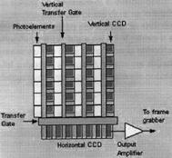 Full Frame
Similar one to the previous one is an architecture much, if it differentiates some because two matrices are had, before it is fotosensibile while the second one is shielded and has the memory function, in fact to the term of the exposure to photons every column of packages of loads comes made to slide in the below matrix in approximately 0,5ms, comes here then transferred to the interface with the same modality that has in the case of the Full Frame Transfer. The advantage is to reduce the interval of time between two successive exposures in how much while the fotosensibile matrix comes exposed to photons, the matrix image comes transferred to the computer, that as before it happens in a time of 100ms.
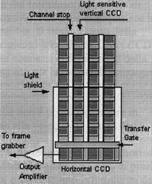 Interline Transfer
In this architecture next to every fotosensibile column a shielded CCD to vertical sliding is had, to the term of the exposure, the Gate transfer qualifies the sliding in it of the packages of loads which come then transferred line for line to the interface. Since it is necessary a shift of a single position, it is had in any case that the successive exposure can happen after approximately100m s, but the complete reading of the sensor happens in approximately 100ms.
5c) Rooms to colors
Sensors CCD are not in a position to give information to us detailed on the frequency and therefore on the color, but only on the brightness of a source, in order to obviate to the problem sin from the primordi of the photography it is rerun to technique RGB of additiva synthesis that consists in the decomposition of the color in the primary colors, in short given an image must some extract red, green and blue the members chromatic.
Various techniques exist in order to obtain this decomposition, are gone from most economic but less effective that it previews I use it of a single CCD until to most expensive in which a CCD for every primary color is used, they come shortly described subdividing them based on the CCD number use you.
1 CCD Room
The method simpler than to use a single CCD is to carry out 3 exposures, with the green filter, with the red one and the last one with the blue, the obtained images come then added, draft of a little efficient method in how much are necessary that the image is very firm during the 3 exposures. An alternative consists in every associating to pixel of matrix CCD a various the following microfilter RGB according to outline:
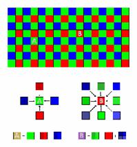
For every point it is famous one of the primary colors while the others 2 can as an example be obtained interpolando relative the chromatic members to the pixel adjacent obtaining the colors of the pixel To and B in figure.
The microfilters greens are the double quantity in number regarding the red ones and to the blueta in how much the human eye introduces the maximum of the sensibility just in the region of the green.
In order to reproduce the image it is necessary to rerun to the interpolation software whose effects are not always optimal therefore come in used kind an alternative outline that diminishes it, in particular use a CCD constituted from pixel rectangular of equal dimension to the half of the points image that are wanted to be acquired,
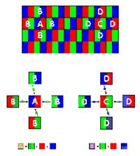
in such a way of every pixel two primary chromatic members while from the 4 pixel adjacent information can be obtained on the shown chromatic member lacking therefore like in figure for the pixel To and C are notes.
2 CCD Room
The resource to the interpolation can be diminished ulteriorly using two CCD,
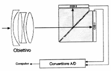
one of the two is filtered in green in how much like saying is the chromatic member more important for the applications dedicated to the human eye, while according to CCD it is leaked with the others two chromatic members,
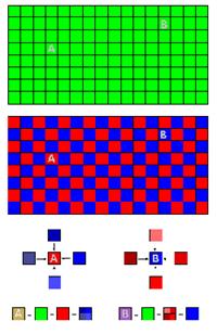
therefore of every point 2 chromatic members while third the outline shown in figure for the pixel comes second obtained for interpolation To and B are notes.
3 CCD Room
Using 3 CCD it is not more necessary to resort to the interpolation in how much to every CCD comes applied a relative filter to a various chromatic member, draft of a configuration much onerosa but that it supplies the best ones turns out to you from the point of view of the quality, and sure it will be in future the most used in how much the cost of the CCD stà quickly diminishing, the realizzativo outline is following:

The applications space them, but also military and trade have demanded them in the years an improvement of the characteristics of the CCD, to leave from the sensitive area for which it is joints a 2048 x 4096 pixel every from 15mm, moreover such sensors can be re-united to form a mosaic so as to to cover greater areas like demanded from the astronomical applications.
In order to reduce the current of buio it has been developed the Fines Pinned Phase (MPP) CCD which one distinguishes from the traditional CCD for a particular polarization of the electrodes and a impiantazione of Boron under one of they, unfortunately this technique reduces the "hole of upgrades them",
and therefore the saturation, of approximately 60%.
For being able to improve the answer in the UV and also in the X in one CCD of the forehead-illuminated type, it is
be developed of recent one technical that is known like the "Open Electrode" or also
"Open Phase", that one of the 3 electrodes consists in discovering, and in correspondence of such
scopertura to implant Boron atoms, so as to to obtain a hole of it upgrades them also without
electrode. Cancellation UV and X that arrive from the part of the electrodes (being forehead-illuminated), do not come absorbed from the third electrode, and therefore it can generate loads.
In order to reduce the noise of reading introduced from the escape stage, it has been developed Skipper CCD which measure loads contained in pixel many times without to right y it, in such a way the measures come "mediated" on the escape amplifier.
